Jump to a section below:
Most important in the testing of any component for frequency response over 100 MHz is a good Network Analyzer and carefully designed test fixtures for calibration as well as for the actual testing. The same is true when testing in the time domain. When measuring rise time characteristics, one must be aware of overshoot and undershoot of the rise time pulse that may affect the signal quality adversely.
Fixture design starts with suitable SMA connectors on high frequency board material. There are several materials suitable for this including FR-4, G-Tech materials, and
several Rogers PCB materials. Many feel FR-4 material is suitable since the fixture zeroing process will eliminate its high frequency loss characteristics. As a general rule, below 6 GHz is okay; above 6 GHz use of Rogers high frequency circuit materials such as, RO3203 or RO4350 will improve the test performance. Rogers has several other materials available depending upon the TCE matching of the component/s or performance requirements. Most of these materials are ceramic filled.
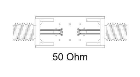
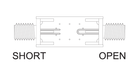
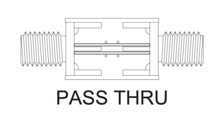
Figures 6, 7, 8 and 9 below show calibration board layouts for a shorted to ground, and open circuit, through line transmission, a 50 Ohm impedance termination, and the layout used to test the device. As many ground points as possible were used along with avoiding and sharp corners. All signal path transitions were made as gradual as possible.
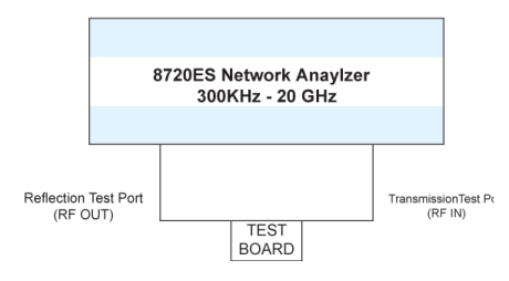
Once the calibration testing was completed, our test process was as follows using an Agilent Network Analyzer Model number 8720ES (See test layout in figure #4).
All calibration boards were entered into the network analyzer and stored. The relay under test was then measured and stored. The calibration data was then entered and
the losses due to the board under the various configurations was extracted yielding the results shown below. This was compared with data extracted from a MIMICAD pro-gram using the equivalent circuit presented and the S parameters; and it was found both tracked very closely.
See the results from the data shown below taken from network analyzer. Included are the isolation, insertion loss, and VSWR. Also, included below is a Smith chart indicating the impedance for a given frequency over the entire frequency range.
Fixture Design
Definition of the exact geometry your test fixture will take is the first key step. Listed below are four geometries and their corresponding equations for calculating the
characteristic impedance.
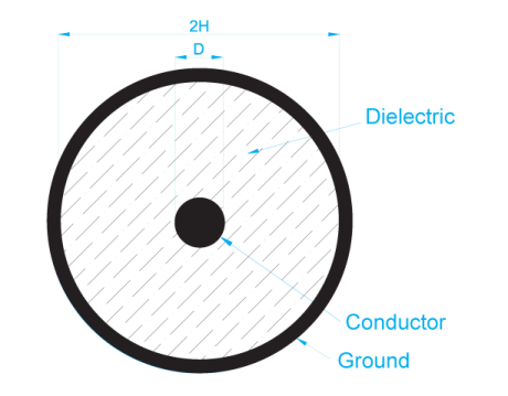
Zo = 60/(√ (εr)) ln ((2h)/d)
Equation #5 (for a coaxial cable)
Where h and d are defined above and εr is the dielectric constant for the material between conductors.
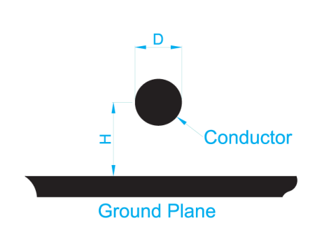
Zo = 60/(√ (εr)) ln ((4hkp)/d)
Equation #6 (for a round wire over ground) for a round wire over ground
Here kp is the proximity factor for round wire over ground, which is near unity when the ratio h/d is large; but for close spacing is approximately
kp = ½ + (√ (4h2 – d2))/4h
Equation #7
kp is reduced to ½ when the round wire touches the ground at d = 2h. The proximity effect results from the same mechanism as skin effect. Mutual repulsion drives like currents to the extreme outer edges of individual conductors carrying current in the opposite direction. This crowds the current in round wires toward the side nearest a ground. As is the case while signal is going through the relay, the proximity effect and skin effect are indistinguishable for a coaxial line because the entire surface of the round center conductor is at the same distance from the shield. Proximity effect is not normally considered for thin rectangular conductors, but skin effect does drive the currents toward the edges of the conductors.
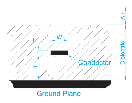
Zo = 60/(√ (εr)) ln ((5.98h)/(0.8w + t))
Equation #8 (buried microstrip over ground)
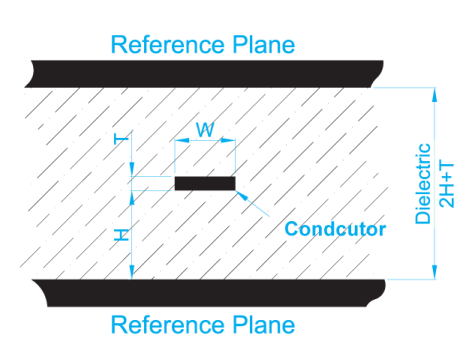
Zo = 60/(√ (εr)) ln (3.8(h +0.5t)/(0.8w + t))
Equation #9 (Stripline between ground planes)
Test Setup and Test Fixtures
Key to the proper testing of a component in an RF circuit is the proper use of test fixtures.
Calibration Approach Critical
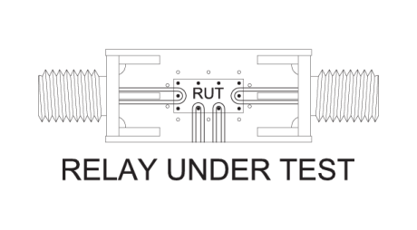
The fixtures were constructed to serve as calibration boards to allow for better characterization of the relays. All the fixture boards used to test the relays under test (RUT) used SMA connectors for connection to and from the test equipment and for terminations. The following are the makeup of the boards under test:
- RUT calibrated with a 50 Ohm line and open termination
- RUT calibrated with a 50 Ohm line and shorted termination
- RUT calibrated with a 50 Ohm line and 50 Ohm termination
- RUT calibrated with a 50 Ohm through line
Test Results
Figures #10 through 16 represent the results of our testing using the procedures previously described and the fixtures presented. The fixtures used were made from
FR-4 printed circuit board material. Improvements to the fixturing, using some of the Rogers PCB material may improve the results.
Insertion Loss
As explained earlier, insertion loss is the loss of power going through the relay. Insertion loss is one of the most important measurements in RF because it is simply a measure of the loss of the signal going through the component (Reed relay). Minimizing this loss is a key interest.
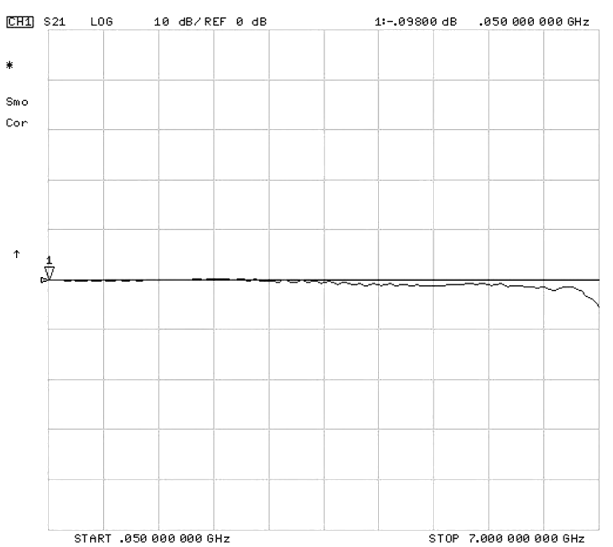
First, it can be clearly seen that the insertion loss looks excellent up to 7 GHz, as shown in Figure # 10. As shown, the insertion loss curve is very flat and begins to tail off at 7 GHz. Clearly, this indicates signals, whether digital or analog, will fare very well when switched and passing through this CRF ceramic Reed relay. When using semiconductors as a switching element, intermodulation distortion may sometimes occur, giving rise to distortions in the frequency response. With a passive device such as the Reed relay, no intermodulation distortion exists, resulting in a very flat insertion loss up to 7 GHz. Having this very flat insertion loss allows the user the ability to switch, carry or deal with a multitude of different frequencies or different width digital pulses, without having
to worry about having different switches to handle the different frequencies.
Copper Wire Insertion Loss

At higher and higher frequencies, it has been proposed that a Reed relay, because it uses nickel/iron as its center conductor, will not have very good performance characteristics. Skin effect is often the proposed culprit, because nickel and iron, being ferromagnetic, have a high magnetic permeability μ. However, this is not the case as shown in figure #11, where the Reed switch in figure #9 was replaced with a pure copper wire.
Comparing figures 10 and #11, one sees little or no difference. Under high power transmission conditions, a difference would probably be seen. But as is the case in many applications, the power being switched is very low; and therefore, we only see a negligible effect up to 7 GHz.
VSWR
mark.
VSWR represents the effects of the transmission of power due to standing waves. When standing waves are present on a line, some power is being reflected back on the line and re-reflecting again from the source. This back-and-forth reflection produces standing waves. These standing waves interfere with the transmission of the original signals from the source because they are continuously present and continually absorb power. Figure 12 presents the VSWR for the Reed Relay. While still an important RF characteristic
for analog continuous wave analysis, insertion loss is looked on more for RF characteristics.
Isolation
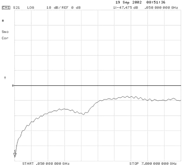
Vertical scale: 10 dB/div referenced from the 0 mark.
Isolation is the ability of a component to isolate the RF signal from propagating further in a circuit. For a Reed relay, the isolation is a measure of the ability to halt further
progress of the signal when it is in the open state. We all think of a switch in the open state as meaning no signal passes beyond those open contacts. However, with RF we know an open circuit is not totally open because the capacitance across the contacts represents a leakage path; and indeed, with high enough frequencies, that’s exactly what occurs. Presented in Figure #13 one can see isolation of –50 dB or greater at low RF frequencies which drops to –15 dB at 3 GHz and continues to a level of –10 dB at 7 GHz. Contributing to this drop off in isolation is the contact gap. Increasing the gap on the Reed switch is very difficult to do because it would require a larger capsule, which would increase the package size. Also, a larger gap will make the switch less sensitive for closure, requiring more coil power. If the isolation is a critical parameter in an application, stringing more than one Reed relay together will help. Also using a ‘T’ switch
or half ‘T’ switch will yield much higher isolations.
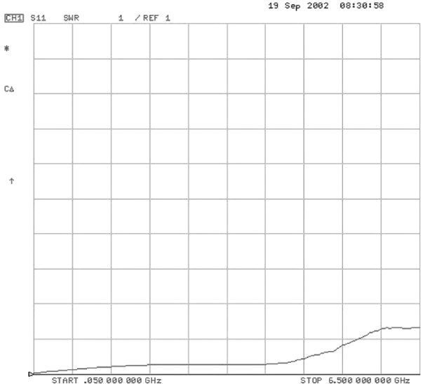
Return Loss
Vertical scale: 10 dB/div referenced from the 0 mark.
Return loss is also an RF parameter that is not used as much as the insertion loss or isolation. As stated, it is a measure of the power of the RF signal being reflected
back to the source. As can be seen in Figure #14, the return loss has only 35 db of reflected signal at the lower frequencies and about 10 db reflected back at 6.5 GHz.
Here the larger the dB level the lower the percentage of the signal being reflected.
Characteristic Impedance
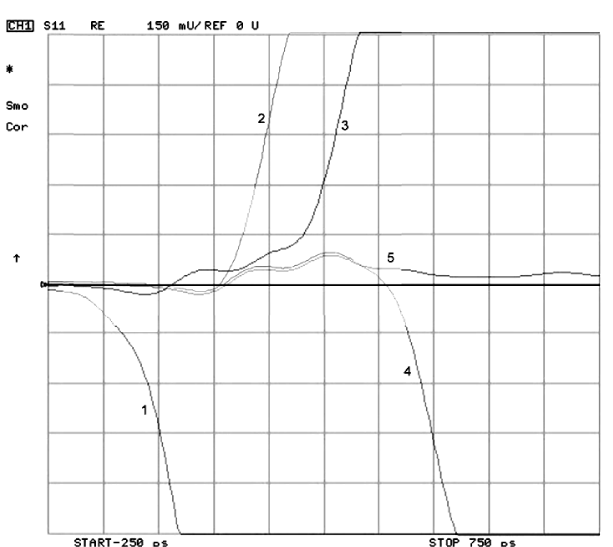
To gain most information from a characteristic impedance measurement of the relay it is fruitful to make measurements of the signal up to certain points while going through the relay. Since this measurement is a spatial measurement, the actual impedance at each point of the relay can be measured. The following points of reference were made as shown in Figure #15:
- A short before the relay defining when the signal enters the relay
- Open contacts define the signal up to the middle of the relay
- Closed contacts define the signal path up to the end of the relay
- Closed contacts with the relay shorted
- Closed contacts with the relay terminate in 50 Ohms
Superimposing the 5 traces on the actual trace through the relay, a full picture of the characteristic impedance can be seen at each point though the relay. This is very
valuable particularly if the relay or component is slightly off the 50 Ohm impedance. As shown in the trace in Figure #15, the relay is slightly above 50 ohms. With the trace being high, this indicates a slightly inductive entrance into and out of the relay. Compensating with a little capacitance on each end of the relay will tune the
impedance to the desired level. This will in turn improve the performance of the relay in a given circuit and increase its performance at higher RF frequencies as well.
Smith Chart
- 1 – Short Before Relay
- 2 – Open Contacts
- 3 – Close Contacts
- 4 – Closed Contacts – Shorted
- 5 – Closed Contacts – 50 Ohm
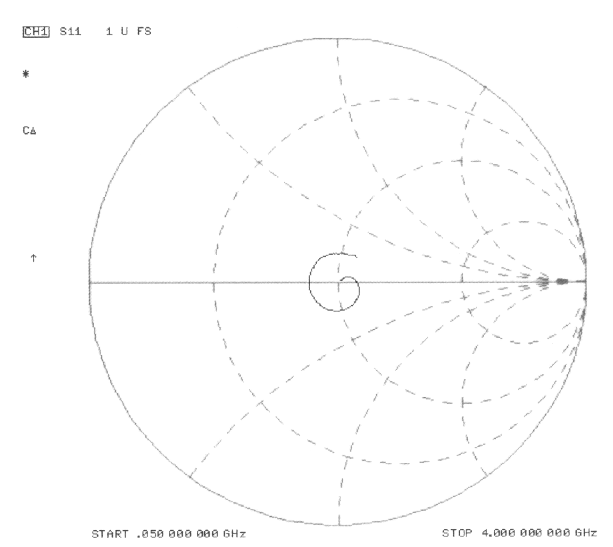
If one is looking at different RF frequencies in a given application or at a specific frequency, a Smith Chart can help by presenting the characteristic impedance over a
given frequency range. The Smith Chart presents a plot of the response of frequencies every 50 KHz up to 4 GHz. Shown in Figure # 16, the plot of points is centered around the 50 Ohm real point. To better understand this Smith Chart, the second dotted circle starting from the right center point of the large circle is the 50 Ohm impedance circle. The center line of the circle running horizontally, is the real axis. Plots above this line are inductive and plots below this line are capacitive. As shown, the plot of the CRF relay is in a tight circle around the real axis and centered around the 50 Ohm circular axis.
.
Summary
As can be seen the CRF Reed relay is an excellent Reed relay for switching and carrying RF signals at least up to 7 GHz and beyond. Our current efforts are to improve its characteristics up to 10 GHz and beyond. This is a reachable goal as we try to continually develop new RF relays, pushing the current bandwidth and current ‘state of the art’. As higher and higher frequencies are used and components are needed to develop these circuits, the need for Reed relays like the CRF series and subsequent improvements on performance over existing data will be needed. Our engineers are up for this challenge!