
Learn how engineers can increase channel density while managing capacitance, crosstalk, and PCB design constraints in modern semiconductor test systems.
If there are particular areas you need help with, feel free to skip to any of the following sections:
- The Challenge: More Channels, Less Space
- Balancing High-Density Design Tradeoffs
- Design the Architecture, Not Just the Relay
- High-Density Switching by Design
- Your Design Partner for High-Density Switching
The Challenge: More Channels, Less Space
As semiconductor devices become more complex, automated test equipment (ATE) and instrumentation platforms are being asked to support more channels within increasingly constrained footprints.
But increasing density introduces new design challenges:
- PCB routing constraints
- Crosstalk between adjacent channels
- Parasitic capacitance
- Signal integrity degradation
- Long-term reliability concerns
The question isn’t simply how to add more channels.
It’s how to maintain measurement accuracy while scaling the architecture.
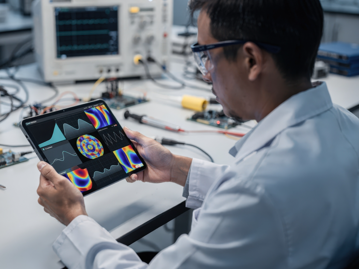
Maintain Measurement Accuracy While Scaling Switching Architectures
Jump to: The Challenge: More Channels, Less Space | Balancing High-Density Design Tradeoffs | Design the Architecture, Not Just the Relay | High-Density Switching by Design | Your Design Partner for High-Density Switching
Balancing High-Density Design Tradeoffs
Hidden Tradeoff #1: Crosstalk
As switching channels move closer together, unintended signal coupling can affect test performance.
The result can include:
- Increased noise
- Measurement errors
- Reduced repeatability
- Lower test confidence
In high-density analog and mixed-signal systems, controlling crosstalk becomes critical to maintaining signal integrity.
Hidden Tradeoff #2: Capacitance
As channel density rises, parasitic capacitance becomes increasingly difficult to manage.
Even small increases can impact:
- Signal fidelity
- Switching performance
- Analog accuracy
- Mixed-signal measurements
The most successful test architectures address capacitance early in the design process, before it becomes a validation issue.
Engineering Insight
As channel density increases, design challenges shift from mechanical constraints to electrical performance. Relay footprint, PCB layout, capacitance, and signal routing must be optimized together to preserve measurement accuracy.
Jump to: The Challenge: More Channels, Less Space | Balancing High-Density Design Tradeoffs | Design the Architecture, Not Just the Relay | High-Density Switching by Design | Your Design Partner for High-Density Switching
Design the Architecture, Not Just the Relay
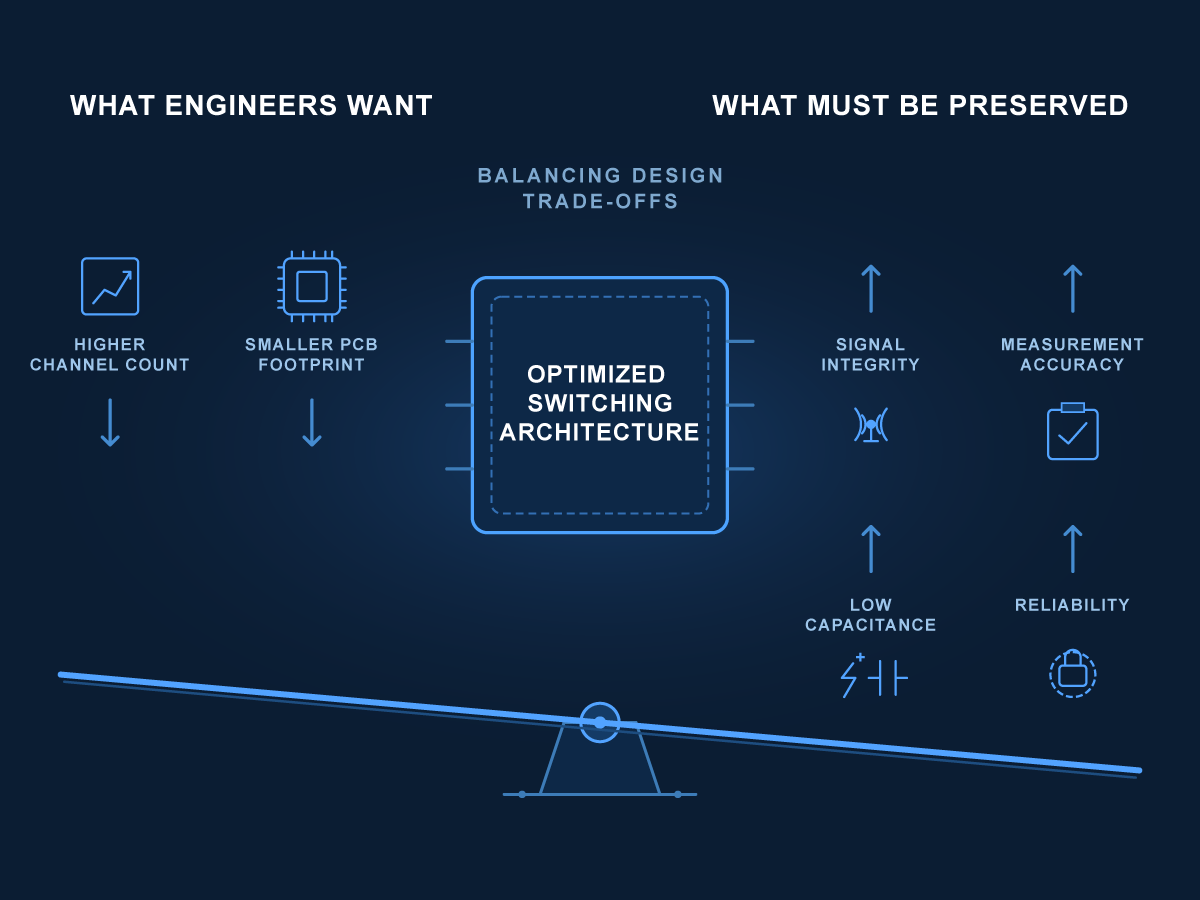
High-density switching requires balancing multiple design priorities simultaneously:
What Engineers Want
- Higher channel density
- Smaller PCB footprint
What Must Be Preserved
- Signal integrity
- Measurement accuracy
- Long-term reliability
Successful switching systems aren’t built around a single component, they’re optimized across the entire signal path.
Jump to: The Challenge: More Channels, Less Space | Balancing High-Density Design Tradeoffs | Design the Architecture, Not Just the Relay | High-Density Switching by Design | Your Design Partner for High-Density Switching
High-Density Switching by Design
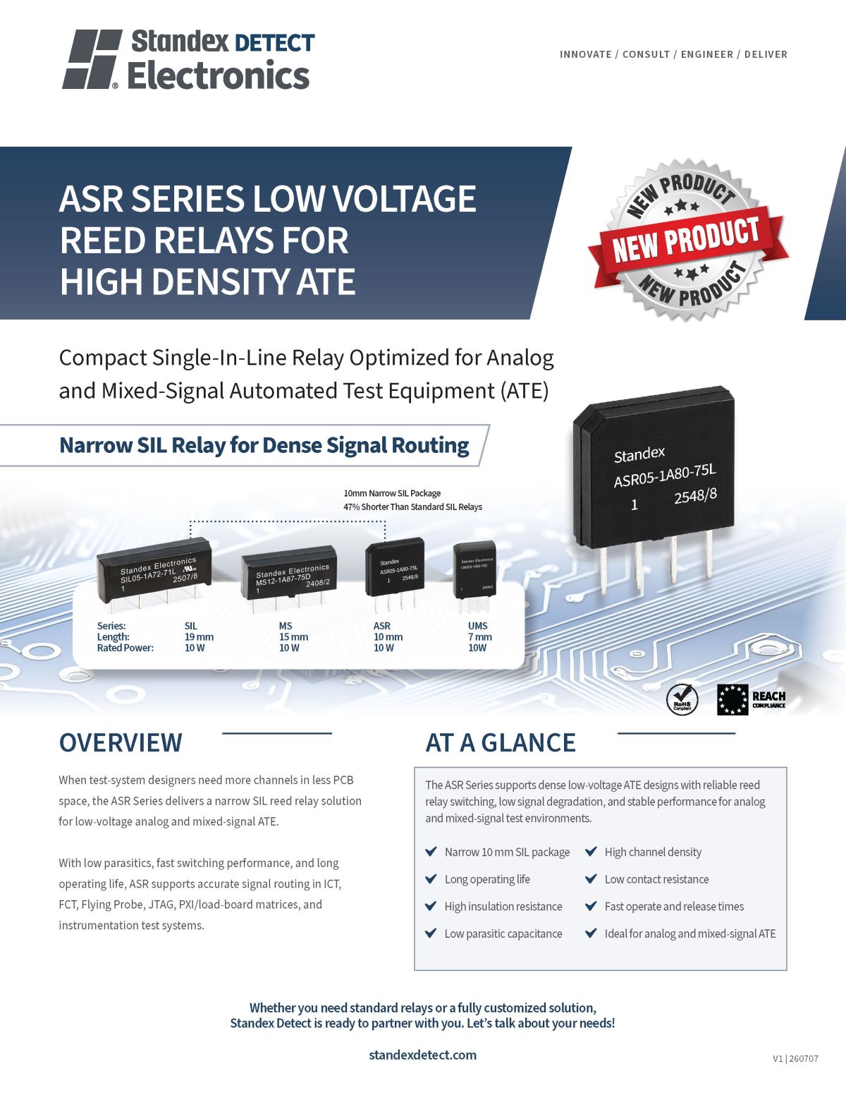
When PCB space becomes the limiting factor, relay footprint and architecture become increasingly important.
The ASR Series features a narrow 10 mm SIL package, 47% shorter than traditional SIL relays, allowing engineers to increase channel density while maintaining low parasitics and reliable signal routing in analog and mixed-signal ATE environments.
Ideal Applications
- Analog & Mixed-Signal ATE
- PXI and Load Board Matrices
- ICT and FCT Systems
- Flying Probe Testers
- Instrumentation Signal Routing
- Data Acquisition Platforms
High-density matrix reed relays maximize channel count in space-constrained test systems. Their compact footprint, fast switching, and flexible stacking options support efficient signal routing for IC test, PCB test, and data acquisition applications.

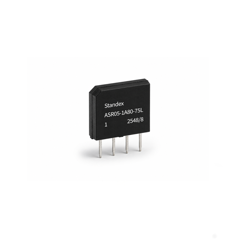
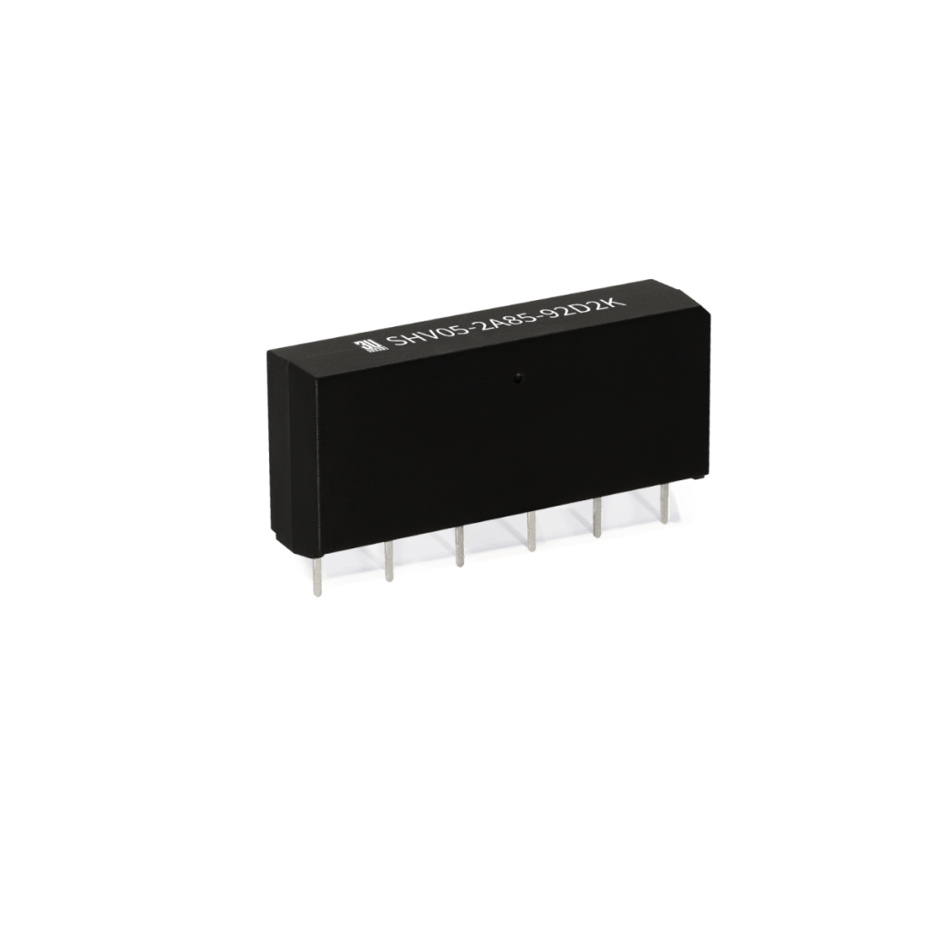

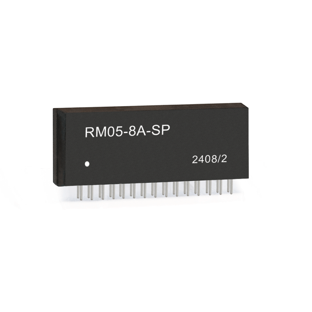
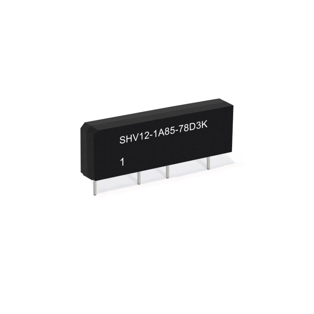

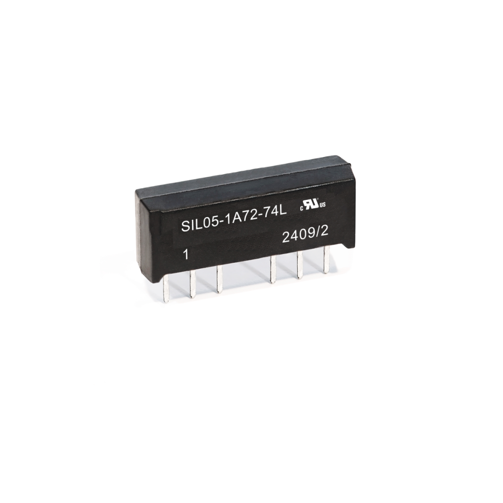

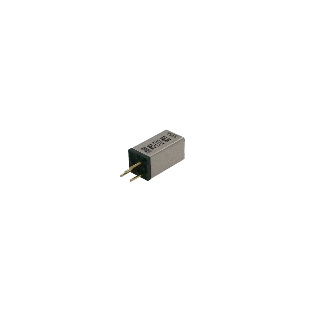
High-density matrix reed relays maximize channel count in space-constrained test systems. Their compact footprint, fast switching, and flexible stacking options support efficient signal routing for IC test, PCB test, and data acquisition applications.
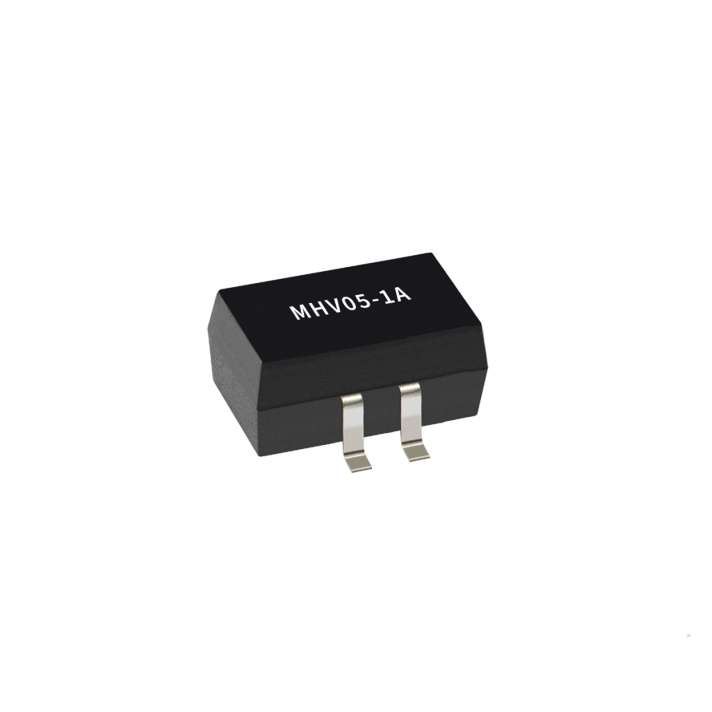
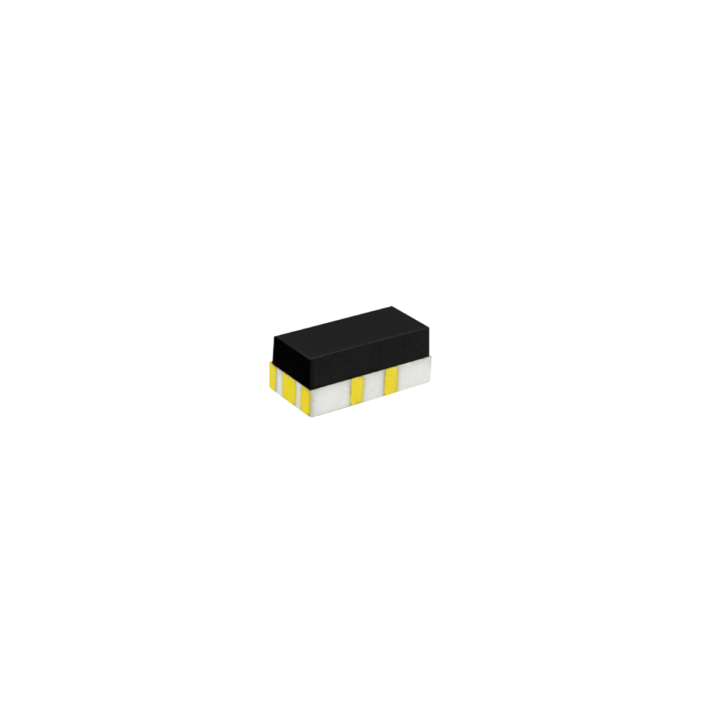

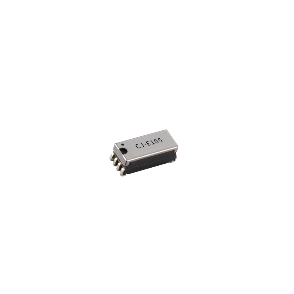
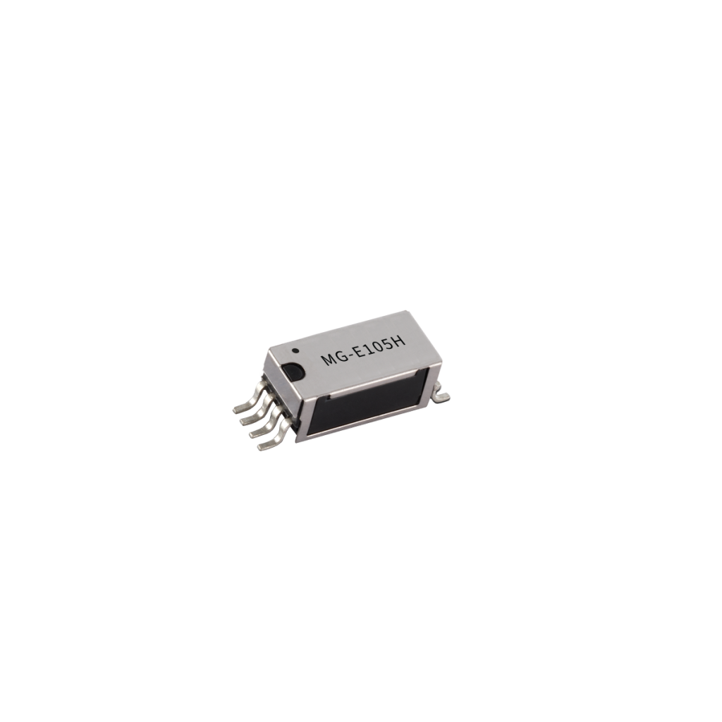
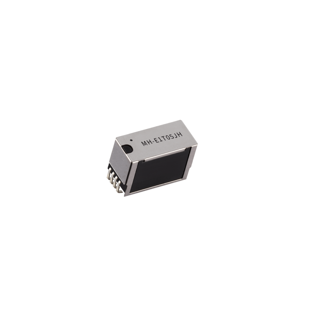
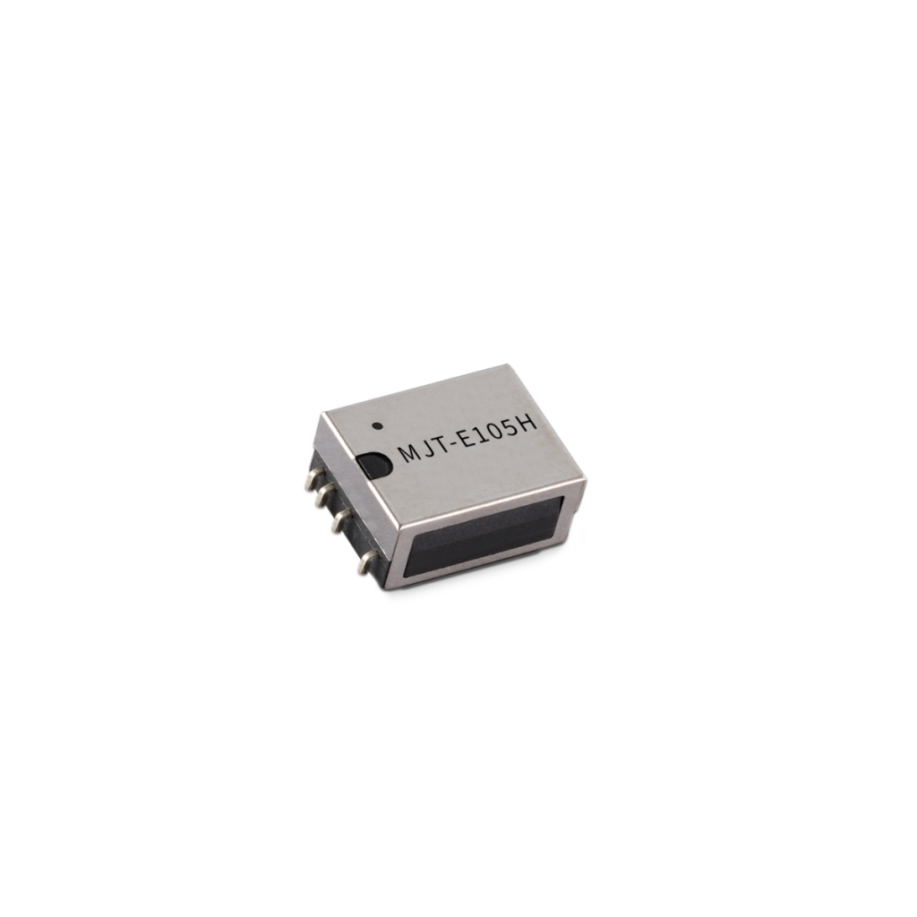
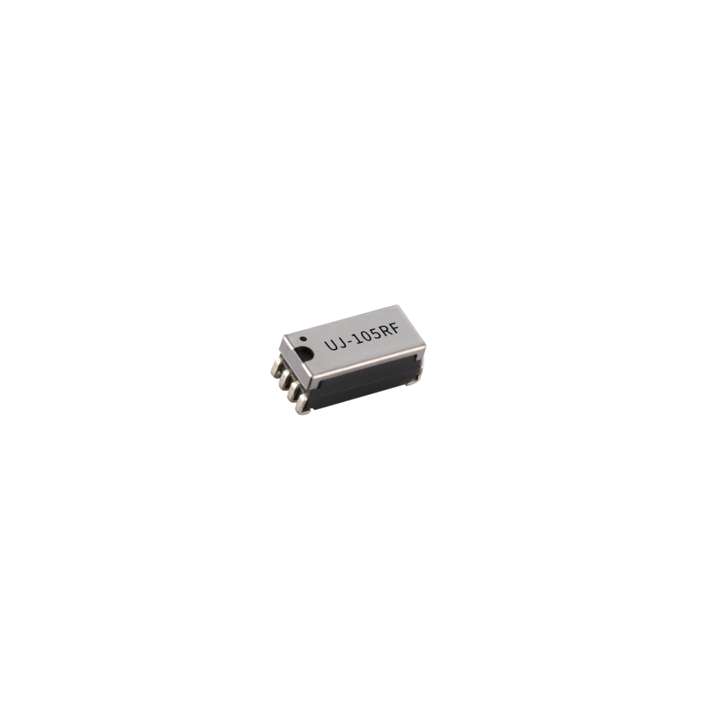
Compact Single-In-Line Relay Optimized for Analog and Mixed-Signal Automated Test Equipment (ATE)
Jump to: The Challenge: More Channels, Less Space | Balancing High-Density Design Tradeoffs | Design the Architecture, Not Just the Relay | High-Density Switching by Design | Your Design Partner for High-Density Switching

Your Design Partner for High-Density Switching
For When it Matters – The Right Design, at the Right Time, at the Optimal Cost.
Standex Detect works directly with engineering teams to optimize switching architectures from concept through production.
By balancing channel density, PCB constraints, capacitance, and signal integrity early in development, engineers can reduce design risk and improve long-term system performance.
The result is more than a relay.
It’s an optimized switching architecture engineered for accuracy, reliability, and scalability.
End-to-End Design
With complete in‑house control from reed switch fabrication to finished sensor assembly, Standex Detect designs, manufactures, tests, and qualifies switching solutions entirely within our organization. This vertical integration ensures consistent performance, stable supply, and faster development cycles, critical for motion systems requiring predictable operation over millions of cycles.
Custom Engineered
Whether utilizing a standard relay platform or a fully customized solution, we work alongside engineering teams to optimize advanced test-system switching.
Global Scale. Application Expertise.
With engineering and manufacturing operations across North America, Europe, and Asia, Standex Detect supports automated test equipment (ATE) and instrumentation platforms from prototype through production. Backed by deep materials science expertise and proprietary lifecycle testing, our switching solutions deliver reliable performance across complex test and measurement architectures.
Co-Engineering Partnership
From architecture development to component selection, we work alongside engineering teams to help increase channel density without compromising measurement accuracy, signal integrity, or system performance.
Talk to Us About Your High-Density System Application
Whether you’re developing a next-generation ATE platform, expanding channel density within an existing test system, or optimizing signal routing in an analog or mixed-signal environment, Standex Detect can help you balance performance and scalability.
What You Gain:
- High-density switching expertise for analog and mixed-signal test systems
- Engineering support from concept through production
- Guidance on density, signal integrity, capacitance, and PCB layout optimization
- Proven relay solutions for accurate, reliable signal routing
- Global manufacturing and supply-chain stability
Related Articles
-

High-Voltage Insulation Monitoring for Next-Generation BESS
Learn how insulation monitoring helps improve safety, reliability, uptime, and asset protection in Battery Energy Storage Systems (BESS). Explore high-voltage monitoring solutions for 1,000–1,500 VDC energy storage applications.
-
When Standard Sensors Aren’t Enough
Real-world applications rarely operate under ideal conditions. Temperature extremes, fluid exposure, vibration, contamination, and limited installation space can all impact sensing performance and long-term reliability. Learn how custom sensor solutions help overcome these challenges and deliver reliable operation in demanding industrial, transportation, EV, agricultural, and energy applications.
-

Reliable Sensing for Safer, More Efficient EV Systems
Learn how reliable sensing supports safer, more efficient EV systems. Explore applications in battery management, charging systems, fluid monitoring, and safety detection and discover how advanced sensing technologies help improve performance, reliability, and operational safety.
-
Eliminating Downtime in Motion Systems with Precision Sensing
Learn how precision sensing helps eliminate downtime in industrial motion systems. Explore real‑world applications in automation, high‑power loads, and fluid‑dependent systems and see how reliable sensing improves uptime and system performance.